Using new materials to explore novel devices
Electronic, photonic, spintronic and sensing

The Koester NanoDevice Laboratory (KNDL) investigates new solid-state device concepts spanning multiple material platforms and applications. The lab works on advanced electronic devices, including scaled metal-oxide-semiconductor field effect transistors (MOSFETs) for end-of-roadmap ultra-large scale integration (ULSI) microchip applications, novel memory devices, high-speed transistors, diodes and varactors, optoelectronic devices, and ultra-wide bandgap semiconductors for high-power electronics.

Two-dimensional (2D) material devices
KNDL develops high-performance transistors using 2D materials for applications in advance logic and memory circuits, as well as optoelectronic, spintronic and sensing devices.
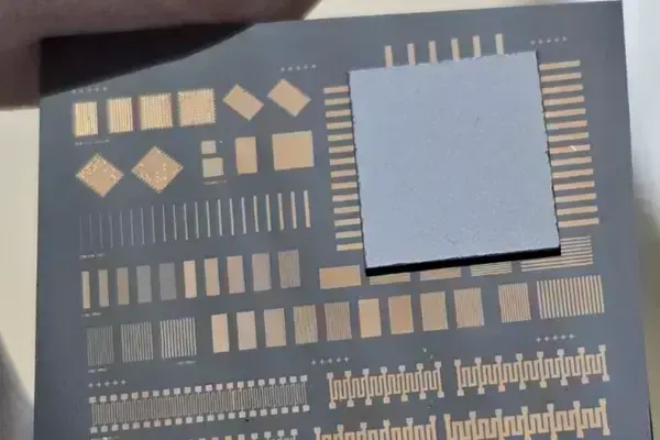
Three-dimensional heterogeneous integration (3DHI)
KNDL investigates ways to use die and wafer bonding to integrate different semiconductor devices to create circuits with enhanced performance.

Ultra-wide bandgap (UWBG) devices
KNDL explores material properties and device applications of emerging ultra-wide bandgap materials, with a focus on group-IV oxide materials.

