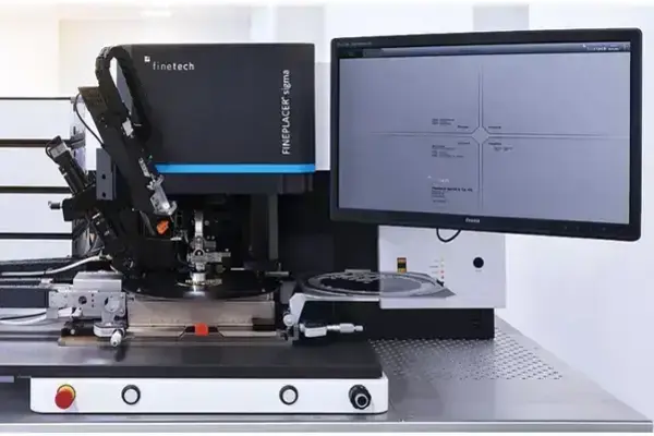
Equipment
The Koester NanoDevice Lab (KNDL) has a full suite of state-of-the-art fabrication and measurement equipment needed to build and characterize emerging nano-scale devices.
-

Agilent 4155C Semiconductor Parameter Analyzer and 4294A Precision Impedance Analyzer
Precision DC and AC characterization of semiconductor devices, including transistors, diodes, resistors, and capacitors.
-

Agilent B1500A Semiconductor Parameter Analyzer
Precision electrical characterization of semiconductor devices, including DC, AC, and capacitance measurements.
-

Agilent 86100B Oscilloscope
High-speed waveform measurement for digital and analog device characterization.
-
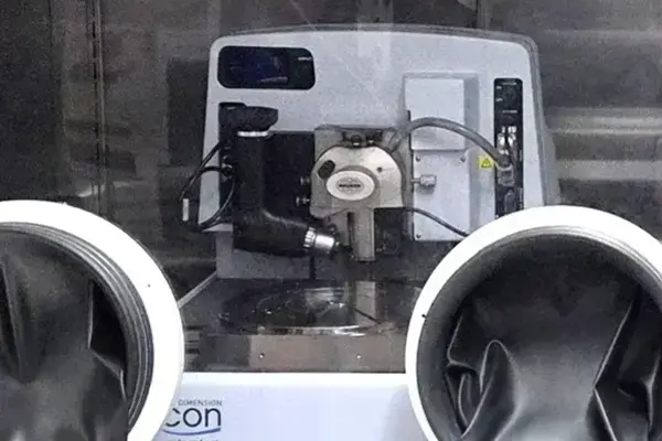
Bruker Dimension Icon AFM (in Glovebox)
Sub-nanometer surface topography measurements for characterizing materials and semiconductor devices.
-

Cascade Microtech Summit 12000 Semiautomatic Probe Station
Semiautomated electrical probing and mapping of semiconductor devices across wafers.
-

Cascade Microtech Summit 11861 Probe Station
DC probing of semiconductor samples across a wide range of sizes and temperatures.
-

Cascade Microtech PLC50 Cryogenic Probe Station
Electrical probing of semiconductor devices at cryogenic and elevated temperatures.
-
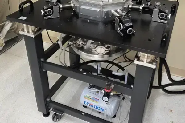
Instec Ultrahigh-Temperature Probe Station
Electrical characterization of semiconductor devices at temperatures up to 1000°C.
-

Keithley 4200A-SCS Parameter Analyzer
Precision electrical and pulsed characterization of semiconductor and ferroelectric devices.
-

MBraun Glovebox
Controlled-environment handling, processing, and storage of air-sensitive materials.
-

Olympus BX51 Optical Microscope
High-magnification optical inspection of semiconductor samples and devices.
-

Veeco Fiji Gen2 Plasma-Enhanced Atomic Layer Deposition System
High-conformality atomic layer deposition of oxide and semiconductor materials with precise thickness control.